

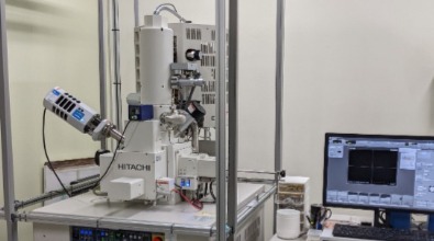
SEM has highly magnification and observes both surface of sample and micro structure of sample (micro section), especially the microscopic analysis of the failed sample. At the same time, the EDS element analysis can speed up the clarification of the possible root cause because of failure occurs.
Major Applications:
- Observation of various material on surface micro structures
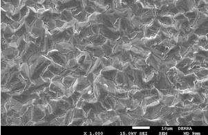
<Tin Lattice of material surface>
- The tin whisker measurement on solder surface of component before and after process assembly
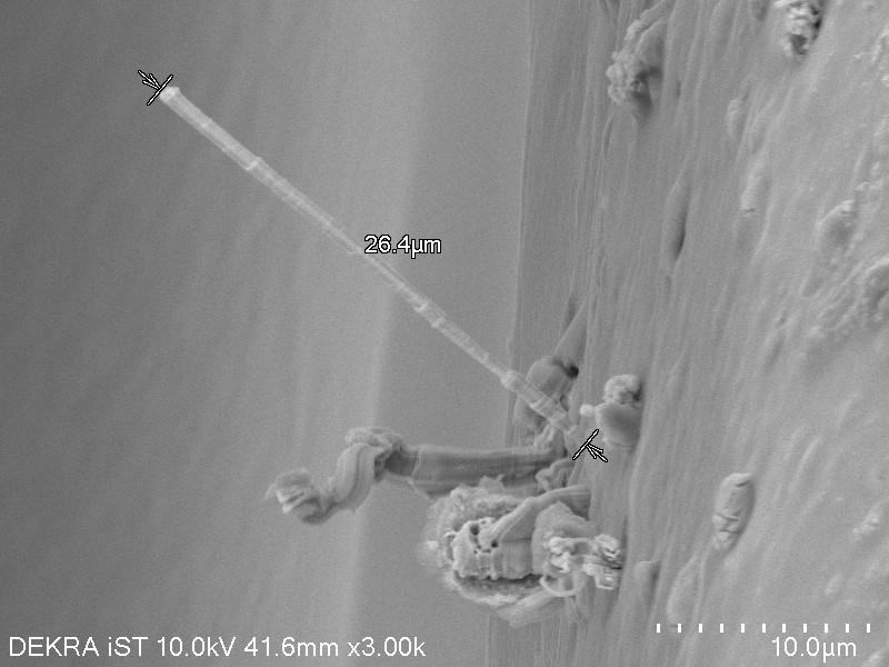
<Tin whisker observation and measuring>
- Plating thickness measurement
- Observation of the component structure or solder joints, such as wire bonding, solder voids, micro-cracks and IMC thickness.
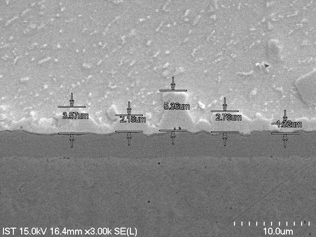
<IMC thickness measurement>
- Surface material analysis by EDS
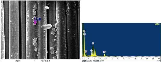
<EDS Element analysis>
To make all your PROBLEMS SOLVED, we provide professional consultant and service.
For more information or service, please feel free to email to 📧 sos@dekra-ist.com


